Olce's Brain Dumpster

    • Contact Me

  • Cell Site Hardware Architecture Part 1

    What is a cell site and why should we care?

    We live in a world where our cellphones are smart enough to do everything we need in order to be up to date with internet memes, chatting, video calls, editing documents with our coworkers/classmates, printing files, ordering something from a website to coding (!).

    Honestly, when I talk to someone, I would be impressed if this person say that they own a PC that is not being used for video games. I don’t really play video games, never got into it. I have this addictive behavior where if I start something fun, I won’t stop doing it until I throw up – hence I quit most of real-time chat programs (such as Internet Relay Chat), or playing video games.

    Back to cell site topic. Our phones play important role in feeding our addiction with the FOMO culture. We want everything fast and faster and in real-time if we could. What is the difference between Micro seconds and Nano seconds anyway? We need to go faster than that. Pico seconds delay is unacceptable!


    Sorry I went off tangent again with cell site. So, as a hardware architect, we have to figure out the latest and greatest hardware we need to put in a cell site so it could radiate the best and fastest technology so your phone could do a “handshake” and benefit from those technologies and by having appropriate hardware/software architecture so you could send the memes to your friends faster than a speed of light.

    Can you be more obvious, please?

    You probably heard about electromagnetic spectrum. It is a complete range of all of types of radiation in our universe. You might be familiar with the term of Infrared, Ultraviolet, Microwave, Gamma Rays, etc. However, not all of the electromagnetic waves are dangerous for us. Some of the waves are visible, some are not – it’s all depend on the range of frequency and wavelengths.

    Protips: The higher the frequencies, the more dangerous they usually are. Higher frequency related to the wave length itself. High Frequencies means shorter wavelengths and the waves does not propagate nicely, meaning you have to be super close to it to get radiated.


    Based on the diagram shown above, we can see how the wavelengths/frequencies are divided into several categories; Radio, Microwave, Infrared, etc. If you pay attention to the wavelength, right side of the arrow corresponds to long wavelength, and left side of the arrow corresponds to short wavelength. As I mentioned above. Short wavelength = high frequencies = does not propagate for shit = danger, more damaging.

    Now when we talk about smartphones, cell sites, memes and stuff. We are talking the range of electromagnetic spectrums from Radio to Microwave. Which roughly from 600MHz to 300GHz. In Telecom world, we called those FR1 (Frequency Range 1 = less than 6GHz) and FR2 (Frequency Range 2 = 6GHz – to 300GHz).

    As operators (see T-Mobile, Verizon and AT&T), guess where they spend their most money on? They would spend BILLIONS on purchasing Electromagnetic Spectrums from the FCC. For these operators, they only interest in 600MHz – 300GHz. So say, T-Mobile has license to majority of 2.5GHz (Band 41) spectrum (up to 180MHz Bandwidth), then T-Mobile customers will get the best experience to browse their internet with the speed that 2.5GHz B41 provided. It has nice propagation and decent capacity/speed.

    Behind the scene, what did the engineers do with the license to specific electromagnetic spectrum? How did they translate that to best customers experience with fast and faster 5G technology?


    I’ll post more! Time for some midnight ramen.
    May 30, 2023
    5G, Cell site design, electromagnetic spectrum, hardware architecture, telecom

  • Projects and stuff

    Alright, I am back and stuff. A lot of things happened since my last post lol. Still working on 5G hardware architecture stuff. I’d say I would want to move to the software part of that so I can understand deeper on how to marry hardware and software features together.

    I think though, I have few things in mind for me to work on. First thing first, get back to coding because I know I still suck at it. It also doesn’t help that I mostly working on writing standards/specs these days, so yes, forgive me for being rusty.

    Anyways, that is all for now. The fact that I update this today is a small win (for me at least). My next post will be a little Wiki about Cell Site Hardware Architecture. Stay tuned!

    Peace, love, east asian mango (because they have the best mangos)!

    May 12, 2023

  • Life update

    Oh boi, it’s been a year since I updated this site.

    There are lot of things I need to share:

    1. I just graduated from UW with electrical engineering degree. My concentration was in Analog Circuit Design.
    2. I built so many cool things over the year, it helped me to think like a real engineer (thanks to Professor Darling and Professor Rudell)
    3. got a job working on 5G stuff

    Anyways, 5G eh? Long story short, my capstone project that I did remotely due to Covid19, gave me a little insights about 5G. Our team built a homodyne (direct conversion) receiver for 2.5GHz 5G application. And 2.5GHz is actually band41 that T-Mobile got from their recent merger with Sprint (guess who’s working on it now ;))

    High level explanation, the receiver itself consist of 3 main blocks:

    1. Low noise amplifier (LNA)
    2. Voltage-controlled oscillator (VCO) utilized MOS varactors
    3. I-Q mixers

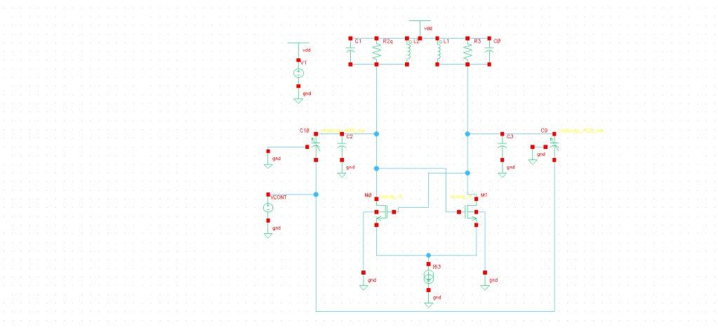
    I personally designed the VCO block. I used an LC tank to set the frequency, some buffer, and frequency divider using D-Flip Flops to produce a 90 degree phase shift that are needed by the I-Q mixers.

    LC oscillator with MOS varactors to vary the frequency
    Frequency divider using D-Flip Flop
    Output from Frequency Divider produced a 90 degree phase shift

    I built these on Cadence Virtuoso Circuit Design Environment, employed with a 65nm CMOS process. However, due to time constraints, we did not build the whole layout for this receiver, someday I will come back to this and finish it.

    Complete Receiver Front-End Schematic

    For the future post(s), I will share the detail on how to build this (the math behind it etc), instrumental amplifier (IA) applications, and I will talk about 5G.

    Can’t wait to blog more.

    Cheers,

    Olce

    September 8, 2020

  • Transmitters transmitters transmitters

    Frequency modulated -> delta amplitude of X(t) gives delta frequency in X'(t)

    Objective:

    15khz FM transmitter in small form factor, preferably capable of 5 watts. Tunable around standard commercial FM ranges, adjacent amateur ranges or similar.

    Maximum deviation: ?? 75khz commercial, 5 khz in LMRS

    The maximum frequency deviation of the carrier is usually specified and regulated by the licensing authorities in each country. For a stereo broadcast, the maximum permitted carrier deviation is invariably ±75 kHz

    https://www.fcc.gov/narrowbanding-overview

    Ideally tunable and in workable range, no high SWR.

    August 2, 2020

  • Eye Diagram Using LFSR

    Heya,

    Unfortunately I am back to school again, but I only have one hard class (designing op amp), and 2 garbage classes, so I probably will continue working on this.

    Last time, I managed to transmit signals over 1000 foot UTP cable. However, to check whether it was garbage signals or not we need to generate eye-diagram to analyze our signals. I had no luck creating appropriate eye-diagram due to the code I uploaded to the Arduino. I needed something that have separate clock and something random.

    Talking about random, I thought about linear–feedback shift register (LFSR). LFSR is a shift register and with a feedback of two or more “taps”. Based on the circuit schematic shown in Picture 1, I tapped bit 0 and 2. You can of course tap more than two, however, there are certain of pattern you need to follow (refer to Picture 2) that can be referred to the length of the loop.

    Picture 1 credit: https://www.eetimes.com/document.asp?doc_id=1274550#
    Image result for lfsr taps table

    Moreover, LFSR would spit out pseudo-random numbers that I need for my eye-diagram testing. The previous set up with Arduino was bad because it spit out constant pattern that of course you can’t analyze whether your signal is bad or not.

    So, I built LFSR with d-flip flop (using TI SN74LS273N), and XOR gate ( HD74LS86 )

    Picture 3: (left) top view of dflip-flop and (right) is pin arrangement for XOR gate

    Using the circuit set up from Picture 1 (a), I use function generator as a clock for the D-flip flop, and output it from pin #6 of the d-flip flop (since I’m only using 2 taps).

    anddddd there she is, the not so pretty eye-diagram (lol). But it’s a progress!

    Picture 4: Latest Eye-Diagram generated using LFSR
    Picture 5: Function generator as a clock for the circuit
    Picture 6: Latest circuit

    October 6, 2019
    Circuit Analysis, Electrical Engineering, LFSR, RS485, Signal Integrity, XOR Gate

  • Fixed schematic and Circuit Board


    The difference between the new one and the previous schematic would be I added 4 120 ohm resistors (R1, R2, R3, R4) from the outgoing side (PIN#9 and #10) of transceiver and incoming side (PIN#12 and #11) of the transceiver.

    So far it looked like I managed to transmit 1Mbps over 1000 foot UTP cables, however at this point I can’t confirm whether the signal I transmitted was smooth or mostly jitters. I still need to figure out how to set up the eye-diagram with external trigger. Will keep you posted!.

    September 14, 2019
    Electrical Engineering, RS485, Signal Integrity, Transceiver

  • Why RS-485?

    Hello people!

    It’s been a while since my last post. I actually did a little summer activities (hiking, gardening, rearranging pantry, making soap etc). BUT I also managed to design the circuit schematic for my serial communication project.

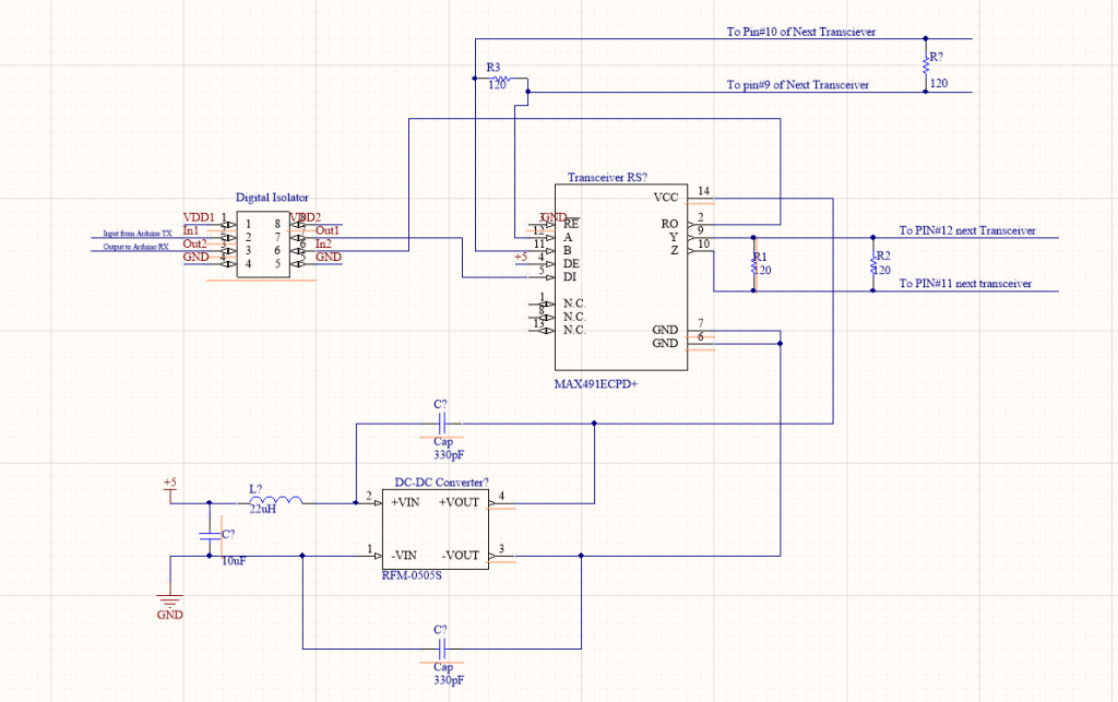
    The schematic as shown in Figure 1 is very drafty. I was using Altium Designer for it, but since I am not making PCB at this moment, I thought this should be doable as my breadboarding reference. Again, this schematic is awful because you can’t really see the flow from the original to the isolation section. I will fix it later!

    Fixed: latest schematic

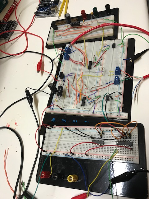
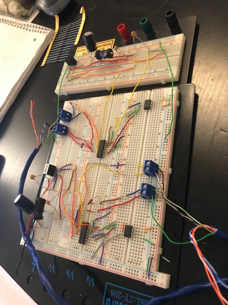
    Breadboarding part I: Look at those loops!

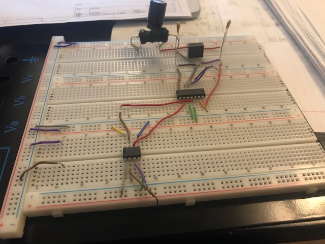
    Figure 2: Bread-boarding based on the schematic from Figure 1

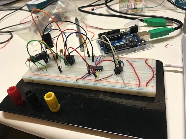
    Then I realized that those loops could introduce unwanted inductance, so I revised.

    Figure 3: Revised breadboard with no loops. Consists of Repeater RS-485, DC-DC converter and Digital Isolator

    As you can see, they look so much better! FLAT. You’d want them flat like that. It’s a tedious work, but I shall get used to it.

    For multigiga serial links (with increasing bitrates), it would suffer from signal distortions. While SerDes receiver designed to compensate those distortions, by creating a bigger eye opening (see: eye diagram) for reliable sampling, the bit rates also rising faster than Rx, PCB, and package HDI. This results in decreasing reachable total channel. RS-485 is a type of repeater that could restore the signals, hence RS-485 extending the channel reach.

    Figure 4: RS-485 (MAX491E) Pin Configuration. Picture credit: maximintegrated.com

    RS-485 use differential signaling over twisted pair, which is beneficial. We know from circuit theory, that differential signaling technique reduces electromagnetic interference (EMI) that could cause cross-talk. In addition, RS-485 also use 3-state logic (1, 0 and high Z) that allows individual transmitter to be deactivated.

    The schematic and circuit board above (see Figures 1,2,3), uses RS-485 as a repeater and it connected it to digital isolator to ensure the power-supply voltage to the MCU is compatible and DC-DC converter to rectify the whole process back to the DC.

    If you notice, the circuit diagram for DC-DC converter contains Inductor(L) and Capacitor (C). The LC circuit is a simple low pass filter to filter out unwanted signals that may present above the wanted pass band.

    So in theory, once we connect all of these out to the UTP cable, 50m cable should not signal faster than 2Mbit/s. We’ll see!

    Will keep you updated.

    Source: https://www.intel.com/content/www/us/en/io/serial-bus-white-paper.html

    August 25, 2019
    Electrical Engineering, repeater, RS485, Signal Integrity

  • Eye Diagram on Oscilloscope

    Heya people!

    It’s been a quiet week, but I managed to review and ordered few things that I needed to get for my on going project. By next week I should be getting my DC-DC converter, Digital Isolator, RS-485 transceiver, and some passive components. I might post the detail on why or how to pick these components to make it compatible to your microcontroller (MCU).

    Further, why did I mention eye diagram on the topic? What is eye diagram?

    Since Signal Integrity is the main topic of my project, an eye-diagram, which is an oscilloscope display (literally it look like an eye), could tell us the quality of serial bit stream and it can be used to debug signal integrity issues. According to Sciencedirect, amplitude noise and timing jitter could impact our system’s performance. However, using simple Bit Error Rate (BER) measurement alone can’t tell the difference between amplitude noise and timing jitter. Eye diagram, on the other hand, provides more information regarding both issues.

    Figure 1: Diagram of Eye Pattern. Picture Credit: sciencedirect.com

    We can take high-bandwidth instantaneous samples of high speed digital signal and the sum of the samples (superimposing ‘0’ and ‘1’) are the eye diagram! To make it more clear, just remember those timing diagram you did in your System Verilog class. The eye diagram would look EXACTLY like one of those state diagrams!

    I was playing with my oscilloscope earlier to display the eye diagram ( I own Tektronix TBS1102B), and unlike the advanced version, I had to manually set up the closest eye diagram I can get from it (see short video below) and I was using high baud rate (2Mbps) to demonstrate the best display of eye diagram.

    void setup() {
      Serial.begin(2000000);
      pinMode(4, INPUT);
      digitalWrite(4, LOW);
     }
    
    void loop() {
        Serial.write(0xAA);
    }
    img_6268

    img_6268

    From this short clip, we can see clearly the transition state from High to Low and so on.

    If you are using the same type of Oscilloscope, this can be accomplished by running code above (connect it with your Arduino, of course), Autoset it, then pick sample (by adjusting the horizontal knob) to the non-static rising edge, then select utility > display > enable persist (to as long as you want).

    ps: I found this artwork (or maybe enlarged screenshot) on Instagram and I want one for my office! lol

    https://www.instagram.com/p/BSE7K2eg8Yu/?utm_source=ig_web_button_share_sheet
    August 16, 2019
    Electrical Engineering, eye diagram, jitter, noise, Signal Integrity, timing jitter

  • Test of Arduino’s USART

    Heya folks,

    Happy weekend to all of you! We had heavy rain on Saturday morning, and it was nice and good for my plants.

    We did a simple linear test with Arduino by using the Tx pin (USART) and to test the highest baud rate it can handle before it introduce some weird stuff on oscilloscope.

    //Again, pin#4 being LOW means for HIGH Z
    //the baud rate in this code is the highest rate that we tested and it had some nasty wave on oscilloscope
    void setup() {
      Serial.begin(2500000);
      pinMode(4, INPUT);
      digitalWrite(4, LOW); 
    }
    void loop() {
       Serial.write(0xAA);
    }

    Baud Rate(Bps)Period ( μs)Frequency(Hz)
    9600~104.29596
    19200~52.0719204
    38400~26.0438402
    76800~13.0276804
    153600~6.512153562
    230400~4.509221778
    460800~2.004499001
    921600~1.002998003
    1843200~0.50121995000
    2000000~0.50111995609
    2500000~0.50141995609

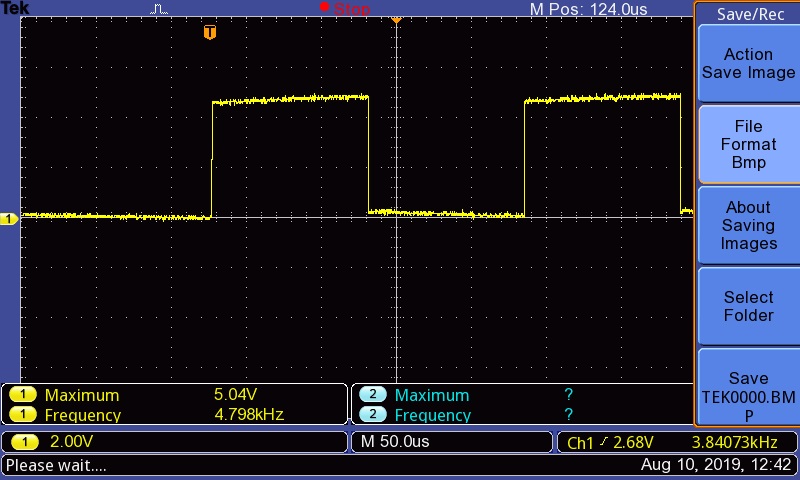
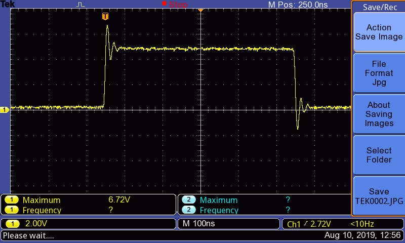
    Based on data above, we noticed that although it maintain the linear behavior, the higher the baud rate (the corresponds frequency value should be very close to the baud rate), the higher the deviation of the frequency rate.

    Check out the screenshots from two different baud rate:

    Period: 124 microseconds
    Period: 250 nanoseconds

    Just by eyeballing those two screenshots, we know that at period 250nanoseconds, the square wave behave abnormally (it has some negative peak, which we don’t want).

    We could say that it is feasible to transmit 1Mbs, BUT definitely less than 2.5Mbs!

    Tomorrow we will use two Arduino to test both Tx and Rx modules. That’s all for now, enjoy the rest of your weekend.

    Also, check out Thom Yorke’s new album:

    Cheers,

    August 11, 2019
    Arduino, Digital, Electrical Engineering, Oscilloscope, Signals, Testing, Transmitting

  • Clock Slips

    Heya folks,

    Few days ago I received my some of the tools for my electronic projects (such as: oscilloscope, Arduino and Multimeter). We (William and I), configured an Arduino to test the oscilloscope by creating a simple square waves. Based on today’s experiment, we accomplished/discovered two interesting things:

    1. Near perfect square wave with no phase shift (117kHz frequency).

    We tested to see the frequency for 50% (no scale) by using analogWrite() function (reference).

    For this configuration, we noticed no phase shift on the analog side of the equation. However, after we tested with digitalWrite() (see reference), we noticed 1/4 of phase shift on our square wave (will update with image later).

    To solve this clock slips/phase shift problem, we did a little research and concluded that one of the reasons of the shift problem is due to interruption on the main (Arduino) code. Hence, we modified the code by adding noInterrupts() (see: reference).

    //The commented code were used to test elimination of phase 
    // shift before using the noInterrupts() function
    //unsigned int usdelay =1; 
    void setup() {
      noInterrupts();
      pinMode(3,OUTPUT);
      pinMode(4,OUTPUT);
      digitalWrite(3, LOW);
      digitalWrite(4, LOW);
    }
    
    void loop() {
      // put your main code here, to run repeatedly:
      digitalWrite(3, HIGH);
      digitalWrite(4, HIGH);
      //delayMicroseconds(usdelay);  
      digitalWrite(3, LOW);
      digitalWrite(4, LOW);
      //delayMicroseconds(usdelay);
    }
    
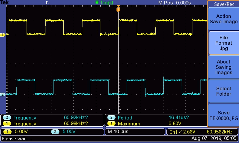
    Figure 1: Output waves on Oscilloscope for two Pins

    For amplitude 5V, we managed to produce desired frequency: 117kHz (1 pin as INPUT) or 60.9kHz (for two pins as INPUT) without phase shift with the noInterrupts() solution.

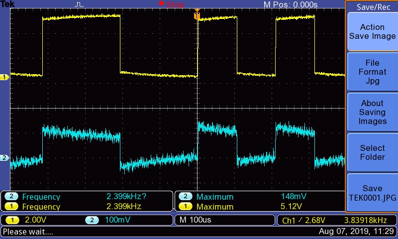
    2. Cross-talk problem using serial connection

    We tested the serial connection with 9600bps and using 0xAA (Binary: 1010 1010 <– you can also imagine this as LOW, HIGH, LOW, HIGH,…, HIGH) pattern, and somehow our configuration introduced a cross-talk problem from the pin#4 we set-up as input (!!!).

    void setup() {
      Serial.begin(9600);
      pinMode(4, INPUT);
      digitalWrite(4, LOW);// pin#4 LOW means High Z
      }
    
    void loop() {
      Serial.write(0xAA);
    }
    Figure 2: Cross-talk issue for serial test

    As we can see from Figure 2, channel 2 (blue) is the square wave from pin#4 and channel 1 (yellow) is the square wave from the serial connection (tx) from the Arduino. We noted that the amplitude of the pin#4 is very low (148mV) compared to the amplitude of channel 1 (5.12V).

    That’s all for today. Will test 2 Arduinos later.

    Peace, Love, Mango

    August 7, 2019
    Arduino, electrical engineer, Oscilloscope, Signal Integrity, square wave

Next Page

Blog at WordPress.com.


Loading Comments...
 

    • Subscribe Subscribed
      • Olce's Brain Dumpster
      • Already have a WordPress.com account? Log in now.
      • Olce's Brain Dumpster
      • Subscribe Subscribed
      • Sign up
      • Log in
      • Report this content
      • View site in Reader
      • Manage subscriptions
      • Collapse this bar